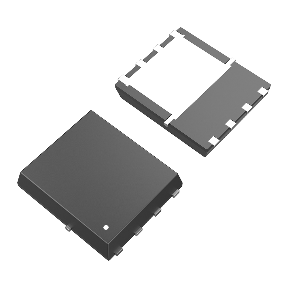
The WSD2090DN56 is the highest performance trench N-Ch MOSFET with extreme high cell density , which provide excellent RDSON and gate charge for most of the synchronous buck converter applications . The WSD2090DN56 meet the RoHS and Green Product requirement 100% EAS guaranteed with full function reliability approved.Advanced high cell density Trench technology, Super Low Gate Charge ,Excellent CdV / dt effect decline ,100% EAS Guaranteed, Green Device AvailableAOS AON6572
Symbol
Parameter
Max.
Units
VDSS
Drain-Source Voltage
20
V
VGSS
Gate-Source Voltage
±12
V
ID@TC=25℃
Continuous Drain Current, VGS @ 10V1
80
A
ID@TC=100℃
Continuous Drain Current, VGS @ 10V1
59
A
IDM
Pulsed Drain Current note1
360
A
EAS
Single Pulsed Avalanche Energy note2
110
mJ
PD
Power Dissipation
81
W
RθJA
Thermal Resistance, Junction to Case
65
℃/W
RθJC
Thermal Resistance Junction-Case 1
4
℃/W
TJ, TSTG
Operating and Storage Temperature Range
-55 to +175
℃
Symbol
Parameter
Conditions
Min
Typ
Max
Units
BVDSS
Drain-Source Breakdown Voltage
VGS=0V, ID=250μA
20
24
---
V
△BVDSS/△TJ
BVDSS Temperature Coefficient
Reference to 25℃ , ID=1mA
---
0.018
---
V/℃
VGS(th)
Gate Threshold Voltage
VDS= VGS, ID=250μA
0.50
0.65
1.0
V
RDS(ON)
Static Drain-Source On-Resistance
VGS=4.5V, ID=30A
---
2.8
4.0
mΩ
RDS(ON)
Static Drain-Source On-Resistance
VGS=2.5V, ID=20A
---
4.0
6.0
IDSS
Zero Gate Voltage Drain Current
VDS=20V,VGS=0V
---
---
1
μA
IGSS
Gate-Body Leakage Current
VGS=±10V, VDS=0V
---
---
±100
nA
Ciss
Input Capacitance
VDS=10V,VGS=0V,f=1MHZ
---
3200
---
pF
Coss
Output Capacitance
---
460
---
Crss
Reverse Transfer Capacitance
---
446
---
Qg
Total Gate Charge
VGS=4.5V,VDS=10V,ID=30A
---
11.05
---
nC
Qgs
Gate-Source Charge
---
1.73
---
Qgd
Gate-Drain Charge
---
3.1
---
tD(on)
Turn-on Delay Time
VGS=4.5V, VDS=10V, ID=30ARGEN=1.8Ω
---
9.7
---
ns
tr
Turn-on Rise Time
---
37
---
tD(off)
Turn-off Delay Time
---
63
---
tf
Turn-off fall Time
---
52
---
VSD
Diode Forward Voltage
IS=7.6A,VGS=0V
---
---
1.2
V
Switch, Power System, Load Switch, electronic cigarettes, drones, electrical tools, fascia guns, PD, small household appliances, etc.